The combinational circuit do not use any memory.
Design a combinational circuit that generates output as 1 use k map for boolean minimization.
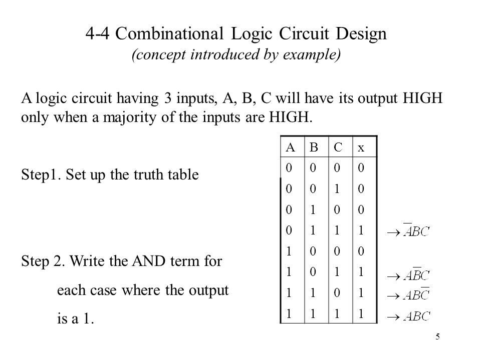
From the design specification obtain the truth table from the truth table derive the sum of products boolean expression.
Example 2 consider the same expression from example 1 and minimize it using k map.
Next you will learn using guided worked examples how to design combinational logic circuits in minutes.
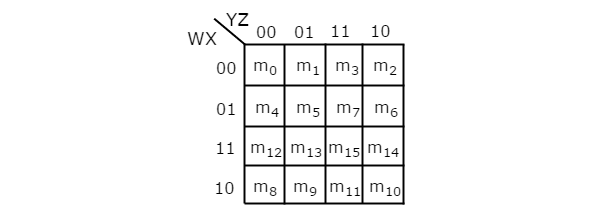
Minimization using k map the algebraic manipulation method is tedious and cumbersome.
The k map method is faster and can be used to solve boolean functions of upto 5 variables.
The simplified boolean function for each output is obtained using k map tabulation method and boolean algebra rules.
Repeated numbers should consider as single number design a combinational circuit that generates.
As you can see the reduced circuit is much simpler than the original yet performs the same logical function.
Use karnaugh map to minimise the boolean.
Combinational logic circuit design.
Draw the logic diagram using the and or gates and discuss its inference.
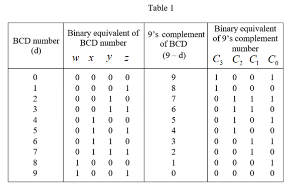
January 18 2012 ece 152a digital design principles 30 combinational design example 1 design specification design a logic network that takes as its input a 4 bit one s complement number and generates a 1 if that number is odd 0 is not odd label the inputs a b c and d where a is the most significant bit.
A combinational circuit can have an n number of inputs and m number of outputs.
The output parity bit expression for this generator circuit is obtained as.
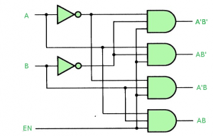
Example of combinational logic circuit.
The logic diagram is drawn.
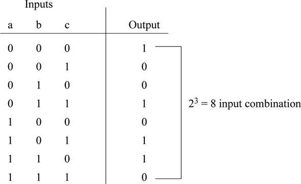
Design a combinational logic circuit with three input variables such that it will produce logic 1 output when one or two the input variables are logic 1 but not all the three.
P a b ex nor c.
Follow the above listed points to design the logic diagram as per the given statement.
The truth table of the odd parity generator can be simplified by using k map as.
The previous state of input does not have any effect on the present state of the circuit.
Questions marks 1 4m design a combinational circuit that generates output as 1 only for particular input pattern student s vtu number use k map for boolean minimization.
Understanding this process allows the designer to better use the cad tools and if need be to design critical logic.
To convert a gate circuit to a boolean expression label each gate output with a boolean sub expression corresponding to the gates input signals until a final expression is reached at the last gate.
Combinational logic circuits design comprises the following steps.
Please refer this link to learn more about k map.
The above boolean expression can be implemented by using one ex or gate and one ex nor gate in order to design a 3 bit odd parity generator.