This combinational circuit has n input variables and m outputs.
Design a combinational circuit with the following input output relationship.
When the binary input is 0 1 2 or 3 the binary output is 1 greater than the input.
Identification and determination of number of available input variables and required output variables.
Find the required number of input variables and outputs from given specifications.
Construct the truth table to define relationship between inputs and outputs.
Combinational circuit is a circuit in which we combine the different gates in the circuit for example encoder decoder multiplexer and demultiplexer.
A combinational circuit can be designed using the following steps.
The following figure shows the block diagram of combinational circuit.
The generated parity bit would be 1.
The logic diagram is drawn.
Simplify the boolean expression for each output.
First ensure that the circuit is combinational that is there is no feedback of an output to an input that the output depends on.
Label all inputs input variables label all outputs output functions.
Each combination of input variables will affect the output s.
The simplified boolean function for each output is obtained using k map tabulation method and boolean algebra rules.
Representing symbols alphabets for each and every input and output variables.
The output would generate the even parity bit for the corresponding input given.
Although the circuit shown in fig.
According to the given specs of the circuit determine the number of inputs and outputs and assign a symbol to each.
Determine required number of inputs and outputs from the specifications.
Expressing the input and output variable s relationship.
2 2 1 does the.
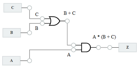
This means that column f and the three input and gate are not needed also the three input or gate can be replaced by a two input or gate.
First of all.
To obtain the boolean expressions and truth tables from the combinational logic circuit we need to analyse the circuit.
Design a circuit which has 3 inputs and a one output with following requirements.
Otherwise output 1.
Some of the characteristics of combinational circuits are following the output of combinational circuit at any instant of time depends only on the levels present at input terminals.
To design a combinational logic circuit use the following procedures.
2 2 2 designed from a boolean equation derived directly from a truth table does give the required output the simpler and cheaper circuit shown in fig.
So we know that when the input is less than 5 z should be 0.
The circuit has 3 inputs as the octal digits need 3 bits to be represented where it would only take the octal digits.
When the input is less than 5 output 0.
Design procedure of combinational circuits.
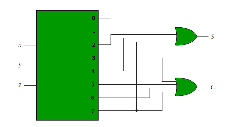
Computer science q a library design a combinational circuit with three inputs x y z and three outputs a b and c.
Derive the truth table for each of the outputs based on their relationships to the input.